Solar PV
SOLAR PV TECHNICAL INFORMATION
The sun releases a huge quantity of energy in terms of human need. Power output per second is 3.86 x 10²⁰ megawatts (MW). This energy fills the solar system, bathing the earth’s atmosphere with a near constant supply of 1.37 kilowatts per square meter. Not all of the direct sunlight incident on earth’s atmosphere arrives at the earth’s surface The atmosphere attenuates many parts of the spectrum; X- rays are almost totally absorbed before reaching the ground, a good percentage of ultraviolet radiation is also filtered out by the atmosphere. While some radiation is reflected back into space, some is randomly scattered by the atmosphere, which makes the sky look blue.
The peak intensity of sunlight at the surface of the earth is about 1 kW/m2. However, not all areas of the earth get the same average amounts of sunshine throughout the year. The most intensely bathed areas lie between 300 north and 300 south latitude, since these areas have the least cloud cover.
Solar PV Principles
Photovoltaic work by directly converting the energy of the sun into DC electricity which can then be converted by inverters into AC electricity for use in a normal electricity grid. Sunlight consists of a stream of photons that contain various amount of energy. This energy can be used to produce electricity through a process using semiconductors embedded in a solar panel. A semiconductor consists of two energy bands of electrons created by using materials with slightly different compositions.
The upper level is known as the conduction band or n-type layer, and the lower level is known as the valence band or the p-type layer. The conjunction between the two layers is known as the p-n junction, and the energy difference at the p-n junction is known as the bandgap. When the semiconductor absorbs a photon of equal or greater energy than the bandgap, electrons will move from the p-type to the n-type layer through a connecting conductor.
This removal of electrons from the p-type layer creates space in that layer which electrons from the n-type layer will fill by flowing through another connecting conductor. This flow of electrons creates an electrical charge difference between the two layers which in turn creates a voltage potential. This voltage potential can be used to produce DC electricity which can then be converted to AC electricity. Photons of lower energy than the bandgap do not produce any electricity, and photons of higher energy than the bandgap will produce electricity, but their remaining energy is converted to wasted heat.
As a result, choice of materials to be used in creating the semiconductor to ensure maximum possible efficiency is important. For a single bandgap, the maximum possible efficiency for capturing the energy of photons is 40% because many photons will either be of too low energy to move any electrons or will be of higher energy than the bandgap, resulting in some wasted heat energy. Theoretically, if photovoltaic cells of different bandgaps were stacked, maximum efficiency could reach 85-90%. As of now, the majority of photovoltaic cells are made with silicon crystals. These cells can reach up to 25% efficiency in laboratory settings but usually only achieve 14-16% in commercial applications. Other materials, including cadmium, indium, telluride, selenium, gallium, and arsenic, have been used in the creation of higher efficiency cells that can reach up to 32% efficiency in laboratory settings. However, many of these materials are toxic and/or rare which means they are unlikely to gain widespread commercial use. Total production can also be improved by using systems that track the sun on either one or two axes Solar cells work best at certain temperatures, according to their material properties: 25 As thermal energy increases,
(i) lattice vibrations interfere with the free passage of charge carriers and
(ii) the junction begins to lose its power to separate charges. The first effect severely degrades silicon’s performance even at room temperatures. The second effect does not
occur until temperatures of about 3000 C for silicon are reached.
As temperature falls, thermal energy is less able to free charge carriers from either dopant atoms or intrinsic silicon. Mobility for light-generated charge carriers drops because they collide more frequently with ionized donors or acceptors. Also, at very low temperature, there is so little thermal energy that even dopants behave as if they were normal silicon atoms.
Components of a PV system
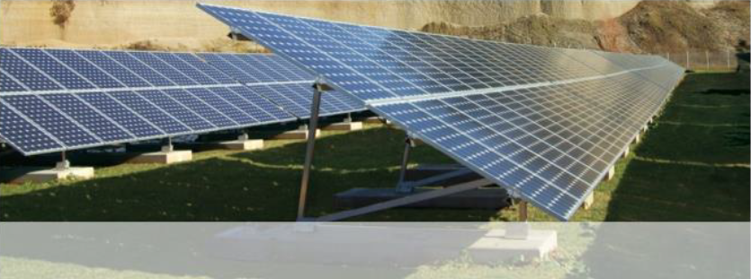
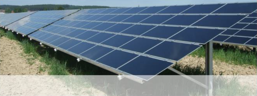
The solar energy conversion into electricity takes place in a semiconductor device that is called a solar cell. A solar cell is a unit that delivers only a certain amount of electrical power. In order to use solar electricity for practical devices, which require a particular voltage or current for their operation, a number of solar cells have to be connected together to form a solar panel or PV module.
For large-scale generation of solar electricity the solar panels are connected together into a solar array. PV modules are then fixed onto appropriate mounting structures and directed towards the sun For PV systems that have to operate at night or during the period of bad weather the storage of energy is required, the batteries for electricity storage are needed.
The output of a PV module depends on sunlight intensity and cell temperature; therefore components that condition the DC (direct current) output and deliver it to batteries, grid, and/or load are required for a smooth operation of the PV system. These components are referred to as charge regulators. For applications requiring AC (alternating current) the DC/AC inverters are implemented in PV systems.
Solar PV cell materials
PV cells are made of light-sensitive semiconductor materials that use photons to dislodge electrons to drive an electric current. The cells may be based on either silicon wafers (manufactured by cutting wafers from a solid ingot block of silicon) or “thin film” technologies (in which a thin layer of a semiconductor material is deposited on low-cost substrates).
Single-crystal silicon is the most frequently used, best understood material for solar cells. Silicon does not exist in a single-crystal form in nature. Rather, it exists as silica, or silicon dioxide, a compound of the two most abundant elements in the earth’s surface. (Almost 60% of the earth’s crust is silica.) A material called quartzite, which can be almost 99% silica in high-grade mineral deposits, is the usual starting point for producing silicon for solar cells. Other materials with a large amount of silicon-such as sand-are not good raw materials because they have too many impurities, which are costly to eliminate. Given the relative abundance and inexpensiveness of quartzite, it is clear that silicon is an attractive solar cell material.
There are two broad categories of technology used for PV cells, namely, crystalline silicon, which accounts for the majority of PV cell production; and thin film, which is newer and growing in popularity.
Crystalline Silicon
Crystalline cells are made from ultra-pure silicon raw material such as those used in semiconductorvchips. They use silicon wafers that are typically 150-200 microns (one fifth of a millimeter) thick.
Thin slices cut from a silicon crystal (in the case of monocrystalline silicon) or from a block of siliconvcrystals (polycrystalline silicon). The main types of crystalline cells in use are monocrystalline, polycrystalline and ribbon silicon. Their manufacture requires a significant amount of energy and raw materials Monocrystalline solar cells are created from a single crystal and are cut from a block of crystal which has only grown in one direction (one plane). Single crystalline is more difficult to manufacturer, making a more expensive option with greater efficiency than the polycrystalline cells. Polycrystalline solar cells are created from a multifaceted crystal which is cut from a block of crystal grown in multiple directions, making them slightly less efficient for the same size cells, meaning having a larger surface area for the same output. Crystalline silicon modules consist of PV cells (typically between 12.5 square cm and 20 square cm) connected together and encapsulated between a transparent front (usually glass), and a backing material (usually plastic or glass)
Thin-film
Thin film is made by depositing layers of semiconductor material barely 0.3 to 2 micrometres thick onto glass, stainless steel or plastic substrates. As the semiconductor layers are so thin, the costs of raw material are much lower than the capital equipment and processing costs. The main types of materials used are:-
Amorphous silicon (a-Si).
Cadmium telluride (CdTe).
Copper indium selenide (CIS).
Copper indium (gallium) di-selenide (CIGS)
The most well-developed thin film technology uses silicon in its less ordered, non-crystalline (amorphous) form. Other technologies use cadmium telluride and copper indium (gallium) di-selenide with active layers less than a few microns thick. In general, thin film technologies have a less established track record than many crystalline technologies.
In amorphous silicon technologies, the long range order of crystalline silicon is not present and the atoms form a continuous random network. Since amorphous silicon absorbs light more effectively than crystalline silicon, the cells can be much thinner.
Amorphous silicon (a-Si) can be deposited on a wide range of both rigid and flexible low cost substrates. The low cost of a-Si makes it suitable for many applications where low cost is more important than high efficiency Cadmium telluride (CdTe) is a compound of cadmium and tellurium. The cell consists of a semiconductor film stack deposited on transparent conducting oxide-coated glass. A continuous manufacturing process using large area substrates can be used.
Modules based on CdTe produce a high energy output across a wide range of climatic conditions with good low light response and temperature response coefficients CIGS is a semiconductor consisting of a compound of copper, indium, gallium and selenium. CIGS absorbs light more efficiently than crystalline silicon, but modules based on this semiconductor require somewhat thicker films than a-Si PV modules.
Indium is a relatively expensive semiconductor material, but the quantities required are extremely small compared to wafer based technologies Commercial production of CIGS modules is in the early stages of development. However, it has the potential to offer the highest conversion efficiency of all the thin film PV module technologies.